General view on calculation of snubber RC-circuits

Igor Vetrov/ Head of operation reliability laboratory
When elaborating powerful transformation sets especially those which work at high frequency, it is necessary to take into consideration the regimes of power semiconductor devices recovery and the voltage surge.
The main way to minimize reverse voltage surge is usage of snubber RC circuits switched on in parallel with powers semiconductor devices.
To calculate parameters of snubber circuits we use dependences which are received as a result of empirical studies which allow to calculate the required parameters accurately enough. To choose accurately parameters of snubber circuit it is necessary to take into consideration inductivity of all the conductors, their constructions and curves of power semiconductor devices recovery in the set operation conditions. It is very difficult to calculate this mathematical model.
We present to your attention the basic model of snubber RC circuits calculation:
Calculation of the snubber capacitor:
Snubber capacitor for phase-control thyristors must overcharge with the charge equal to a half of the reverse recovery charge. At the same time the voltage surge does not have to exceed 80% of the voltage grade of the device.
As a rule value of the reverse recovery charge Qrr for phase-control devices is given for the speed of anode current fall of 10 A/μs
So:
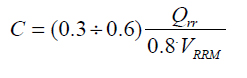
Coefficient 0.3 is used in case when real speed of anode current fall is much less than 10 A/μs.
Coefficient 0.6 is used in case when real speed of anode current fall is close to 10 A/μs.
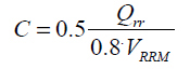
For thyristors which recover with higher speed of fall (for fast thyristors) the Qrr value is taken
for actual speed and the capacity value is calculated the following way:
Formula 2
Calculation of snubber resistor:
Value of snubber resistor resistance is Ñhosen the following way:
- resistor must allow the thyristor to completely discharge the capacitor during the time when the thyristor is conductive;
- speed of discharge current growth of snubber capacitor must not exceed the maximum allowed value of speed of anode current growth ( for reliable work current growth speed from snubber capacitor must not exceed 15÷25% of the maximum value of di/dt);
- value of discharge current of snubber capacitor through open thyristor must be higher than the gate trigger current of the main element; Size of snubber resistor is calculated according to the following formula:
Formula 3
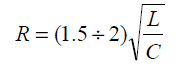 where L is a value equivalent to transformer inductivity.
Snubber circuits must be mounted maximally close to the thyristor.
Inductivity of connecting conductors should be minimized, inductiveless resistors should be used.
Calculation of snubber RC circuits according to the method described above is integration process. Repetitive calculations with corrected input data are necessary to get the results which satisfy all the requirements. Usage of snubber circuits allows to improve working conditions of power semiconductor devices.