Thyristors for Current Impulses Commutation in Amplitude Range of Hundreds kA and Duration Range of Hundreds ?s
Anatoly Chernikov, Vladimir Goncharenko, Alexandr Mizintsev, Dmitry Titushkin and Alexey Surma
Proton-Electrotex, Orel, Russia,
NIIEFA-ENERGO, S.-Peterburg, Russia
Abstract - There was developed a new generation of silicon pulse thyristors adapted for commutation of current impulses with amplitude 100-300 kA, 100 – 1000 µs width. A variety of improvements was done in the layers of silicon structure, topology, and technology of anode and cathode contact generation. It is experimentally proved that commutation of current impulse with amplitude up to 250 kA and 500 µs width by thyristor with 100 mm silicon element is possible.
INTRODUCTION
Development of semiconductor switches able to commute short current impulses with amplitude of tens to hundreds kA is significant for progress in design of pulse power supplies of high power electrophysical equipment [1].
High-spec pulse semiconductor devices used in such switches must meet a number of unique technical requirements, in particular:
- Commutation of currents with rate of growth exceeding 1000 A/µs. Typical requirements are 2000-10000 A/µs.
- Commutation of short pulses of high amplitude currents. Ratio of current amplitude in the commutated pulse to average thyristor current may reach 100 or more.
- Simultaneous engaging of separate devices in a series assembly for commutation of current pulses with high rate of growth.
Pulse thyristors are widely used as such pulse semiconductor devices. However, when commuting impulses with rate of rise of on-state current (di/dt) over 1000 A/µs, significant difficulties occur related to nonsimultaneous switching-on of thyristor element over the whole surface [2-5].
A comprehensive solution for this issue will be using of thyristors with celled «multiemitter» topology used for Gate Turn-Off thyristors (GTO) and Integrated Gate Commutated Thyristors (IGCT) [6], because such thyristor switches almost simultaneously over the whole surface due to small crosswise size of each emitter cell. However for such kind of devices the bigger part of the surface (50% and more) is used to place gate, what significantly decreases the allowed amplitude of current impulse.
Another solution to this issue will be using a special pulse device – Reverse Switching Dynistor (RSD) [7]. Switching-on of such device goes over the whole surface as well, what allows reaching the highest amplitudes of pulse current for the semiconductor switches up-to-date [8]. Nevertheless, there is a disadvantage of this solution, which is necessity to use very complicated equipment needed to launch RSD. Moreover, it costs approximately same price with device.
Thus, it is very important to develop a new engineering solution, which will let increasing allowed pulse current of «conventional» pulse thyristor. Following this introduction there is a set of technological solutions, which allowed developing pulse thyristor able to commute current impulses with extremely high amplitude in important for practical application range of 100-1000 µs.
DESIGN FEATURES AND PRODUCTION PROCESS
Semiconductor layers.
In semiconductor element there is a relatively low-doped p-base (layer resistance under n-emitter 500-1000 Ohm/square). And its dopant profile ensures maximum built-in electric field within this layer. This allows reaching high on-state rate of spread, minimal value of switching delay and drastic decrease in switching delay variations of thyristors in series assembly.
There as well was applied a p-emitter with controlled effectiveness.
In semiconductor element of «conventional» power thyristor there is usually a dependency of n-base thickness (Wn) and values of ambipolar diffusion length of electron-hole pairs in this layer (L) not less than 3 (Wn/L>3). This is determined by necessity to provide the required values of the blocking voltages and dv/dt – sustainability. In on-state, however, distribution of excessive electron-hole pairs over the surface of the semiconductor element is strongly inhomogenous and, as a result, distribution of electric field strength is inhomogenous too.
The p-emitter layer, which is used in the new pulse thyristors, has a limited maximum concentration of dopant impurity. The applied diffusion technologies of its formation together with low temperature technology used to form the anode ohmic contact (sintering) allow regulating its injection rate with very high level of repeatability and getting very homogenous distribution over the surface of the semiconductor structure.
Usage of p-emitter with controlled effectiveness allows lowering Wn/L dependency down to 1 and less. As a result there is a more even distribution of electric field strength over the structure thickness.
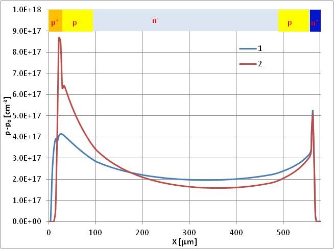
In Fig. 1, as an example, there are results of calculation of distribution of excessive electron-hole pairs concentration and electric field strength with anode current flow of 2000 A/cm2 density for typical thyristors with conventional p-emitter and p-emitter with limited effectiveness. It is clear that electric field strength peak in n-base of the thyristor with limited effectiveness p-emitter is remarkably lower.
(b)
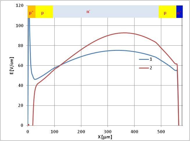
Fig. 1. Typical axial distributions of the electron-hole pairs concentration p-p0 (a) and electric field strength E (b) for thyristor with “conventional” p-emitter (1) and for thyristor with limited effectiveness p-emitter.
Consequently, the thyristor with limited effectiveness p-emitter has a lower corrected local loss power compared to the conventional thyristor with the same voltage drop. When the heat release processes are considered as adiabatic, it allows lowering the local overheat of the semiconductor element for short current impulses down to 20%.
In such a way, energy required for the identical overheat compared to the conventional thyristor for the structure with controlled effectiveness p-emitter is gonna be about 20% higher.
Auxilary thyristor
Pulse power thyristor with big surface of the silicon element and distributed gate (DG) has an auxilary thyristor (AТ), the cathode of which is connected with DG and anode is common with the thyristor structure. AТ purpose is to form amplified gate current pulse applied to DG, which has a considerable length of perimeter. Usually AT structure is formed in a shape of a rather narrow ring, about 1 mm width, which rounds the main gate electrode of thyristor. However, during the commutation of current impulses with rate of rise over 1000 A/µs, density decrease of current flowing through the AТ can go on rather slow. To decrease the density of current flowing through the AT, a so-called distributed AT is applied, which happens to be a «complete» thyristor structure (Fig. 2).
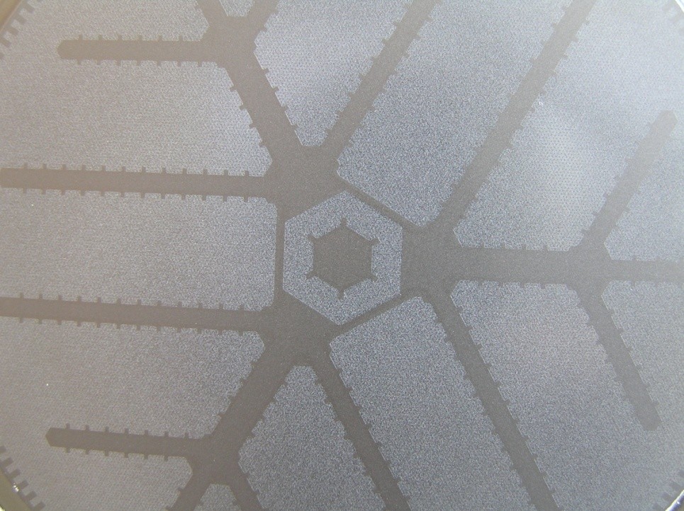
Fig. 2. Distributed auxiliary thyristor (in the center).
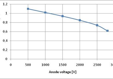
Another factor, which allows decreasing the power loss and overheat of the auxiliary thyristor is a fast drop of current in the AT after switching of the main thyristor. Switch-on delay time of the main thyristor should accordingly be minimized. Usage of the low-doped p-base, described in part A, allows reaching this result. In Fig. 3 there are shown the typical dependency of current and voltage on time during switch-on of the thyristor. It is shown that the dependency of voltage on time has two intervals of rapid drop: the first corresponds to the AT switching-on, and the second corresponds to the main thyristor switching-on. Switch-on delay time of the main thyristor in terms of the AT, which can be evaluated with this curve, equals about 0.7 µs.
Topology of distributed gate.
When designing topology of distributed gate, one of the most important issues can be defining the optimal turn-on time of thyristor over the whole surface (during commutation of current impulses with specified form and width). Computer modelling of electrical and thermal processes during thyristor commutation of current impulse with high amplitude and high rate of rise shows:
- The highest absolute difference of temperature between the hottest spots on the surface of thyristor element (adjacent to gate area) and the coldest spots (most distant from gate area and with the highest switching delay) is reached at the moment of full switching of thyristor over the whole surface. Further occurs a significant (but not complete) flattening of temperature distribution over the semiconductor element surface. The reason for such an effect is positive temperature dependency of peak on-state voltage (VTM): early switched and initially more heated areas, during parallel operation with cooler ones (later switched), conduct current with relatively lower density.
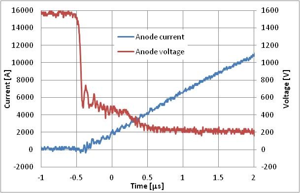
Fig. 3. Typical dependencies of current and volatge on time during switch-on.
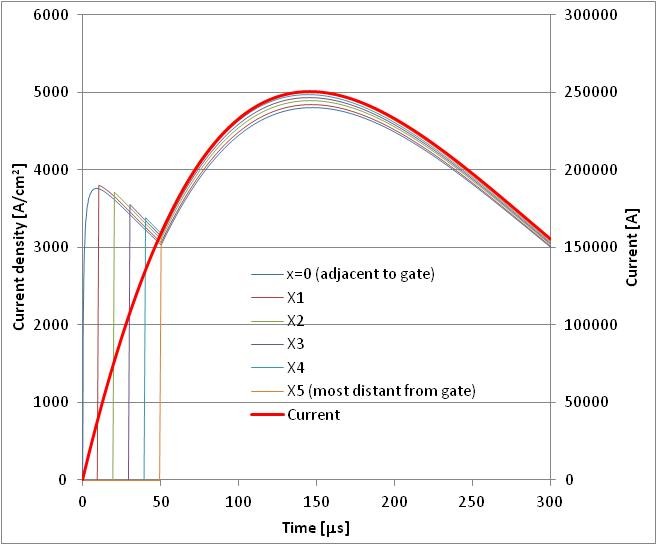
Fig.4. Calculated dependencies of current density on time for the spots of the thyristor structure, which are located at the various distance from the border of the distributed gate electrode.
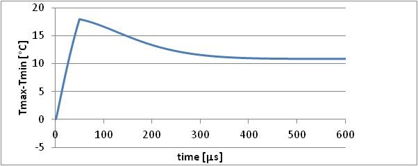
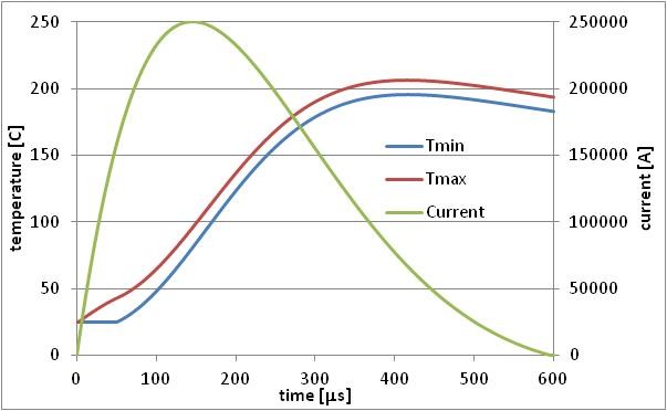
Fig.5. Calculated dependencies of thyristor element temperature during commutation of current impulses with extremely high amplitude.
To reach acceptable low temperature difference over the surface of thyristor element during commutation of current impulses with form close to half sine wave it is enough to ensure full switching of all the surface of thyristor not later the moment, when current of impulse reaches 0.8 of peak value. As an example in Fig. 4 there are the calculated dependencies of current density on time for the spots of the thyristor structure, which are located at the various distance from the border of the amplified gate electrode during commutation of current impulse with 250 kA amplitude and 4000 A/µs rate of rise in initial section. Thyristor element has the following characteristics: 580 µm silicon wafer thickness, 55 cm2 of active surface, 50 µs complete turn-on time. It is clear that current density during the on-state distribution process doesn’t exceed the maximum, which corresponds to the maximum valued of the anode current. In Fig. 5 there are calculated values of temperature of the hottest and coldest spots on the surface of thyristor It is clear that maximum absolute temperature difference on the element surface is about 18°C, and by the moment of maximum overheating of the thyristor element this difference decreases approximately to 11°С, which is just about 6% of the absolute value of maximum overheating of thyristor element.
Contacts.
Anode contact of semiconductor structure with molybdenum disc of thermal compensator made with help of low-temperature sintering by finely divided silver paste [9]. Using it for pulse thyristors can give the following advantages.
- Increase in load-cycling capability. In conditions of short current impulses commutation with extremely high amplitude conduction, each current impulse is followed by very severe thermal cycle for connection of silicon with molybdenum, because silicon is heated up to 200°C temperature, and molybdenum disc, except a fleet layer adjacent to silicon, remains cold. Interlocking joints, result of sintering technology, have very high load-cycling capability [10, 11].
- Increase in load-cycling capability. In conditions of short current impulses commutation with extremely high amplitude conduction, each current impulse is followed by very severe thermal cycle for connection of silicon with molybdenum, because silicon is heated up to 200°C temperature, and molybdenum disc, except a fleet layer adjacent to silicon, remains cold. Interlocking joints, result of sintering technology, have very high load-cycling capability [10, 11].
- During traditional connection process of silicon with molybdenum disc (silumin alloying) the surface layers of silicon structure are being dissolved with silumin. And after that it is impossible to ensure characteristics identity of anode emitter on the surface of structure. And as a result it is typical for traditional technology to show increased density variance of current over the structure surface. Sintering technology excludes such a disadvantage [12].
To guarantee reliable cathode pressure contact cathode gasket made of molybdenum with special coating is used. The choice was made after long lasting significant investigation and testing of various materials and coatings. The selected gasket ensures high load-cycling capability of the contact, low electrical and thermal resistance, no decalage after continuous operation, including commutation of big volume (over 100000) current impulses with high amplitude.
EXPERIMENTAL RESULTS
The experiment pulse thyristors with 2800 V repetitive impulse blocking voltage were produced using the above described technical solutions.
The thyristors had 100 mm silicon element, which was produced using the neutron-doped silicon wafers with 120 Ohm*cm electrical resistivity and 580 µm thickness. Topology of the gate is shown in Fig. 6. This topology ensures the optimal turn-on time of thyristor over the whole surface during commutation of impulses close in its from to half sine wave with 300-1000 µs width. Moreover, surface losses to alignment of the gate were minimized to about 14%, and the active surface of the thyristor element was about 55 cm2. All thyristors had disc housing.
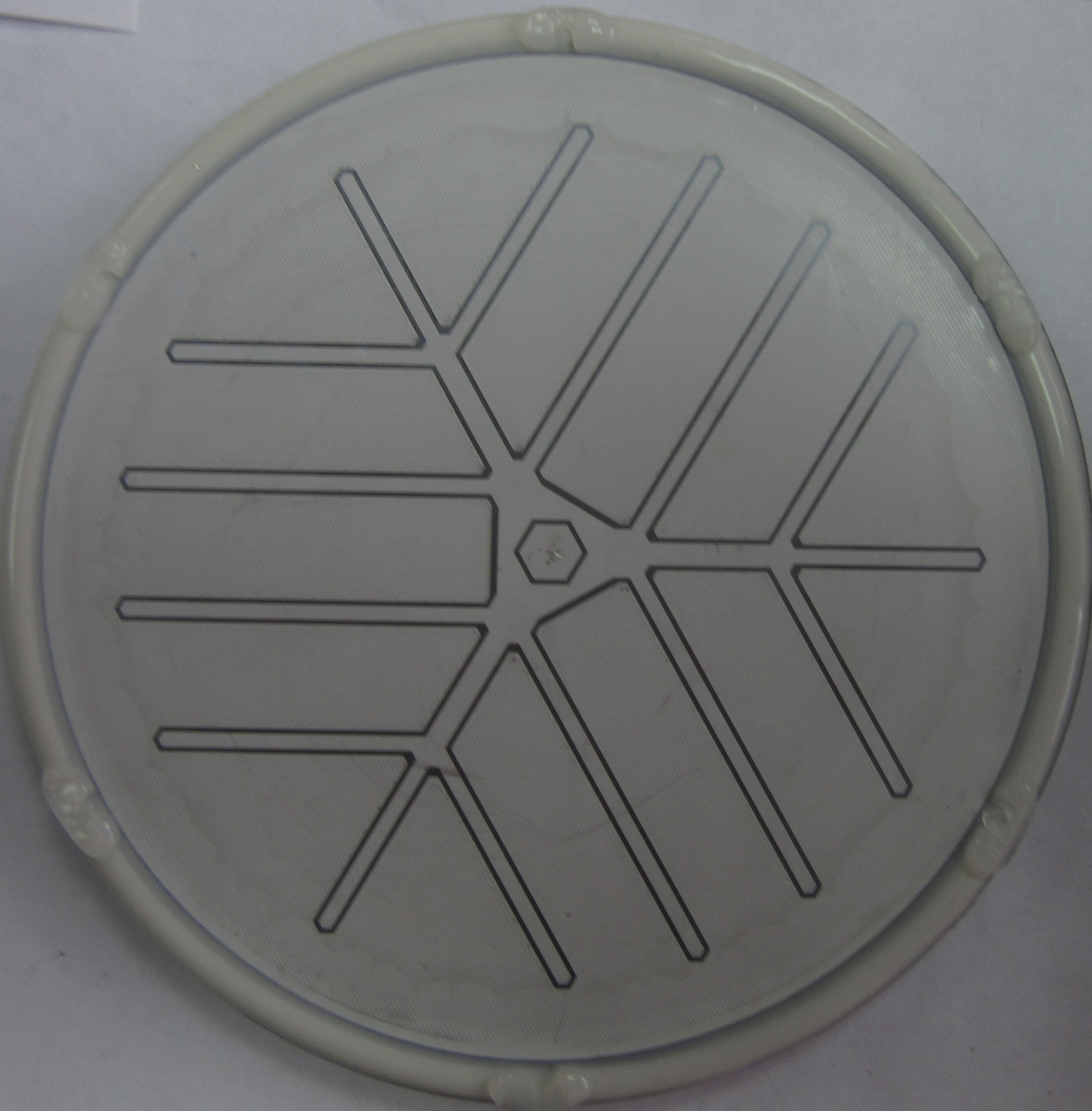
Fig. 6. Topology of thyristor element.
The new thyristors were used to create and test a switch for commutation of current impulses with extremely high amplitude.
The experimental thyristor switch consisted of 10 thyristors in series connection, Fig. 7. The tests were held in R-L-C discharge circuit with 24 kV initial capacitor voltage, Fig 8. The current and voltage impulse forms is shown in Fig.9. During the testing the experimental switch steady commutes current impulses with amplitude up to 250 kA and 4 kA/µs rate of rise.
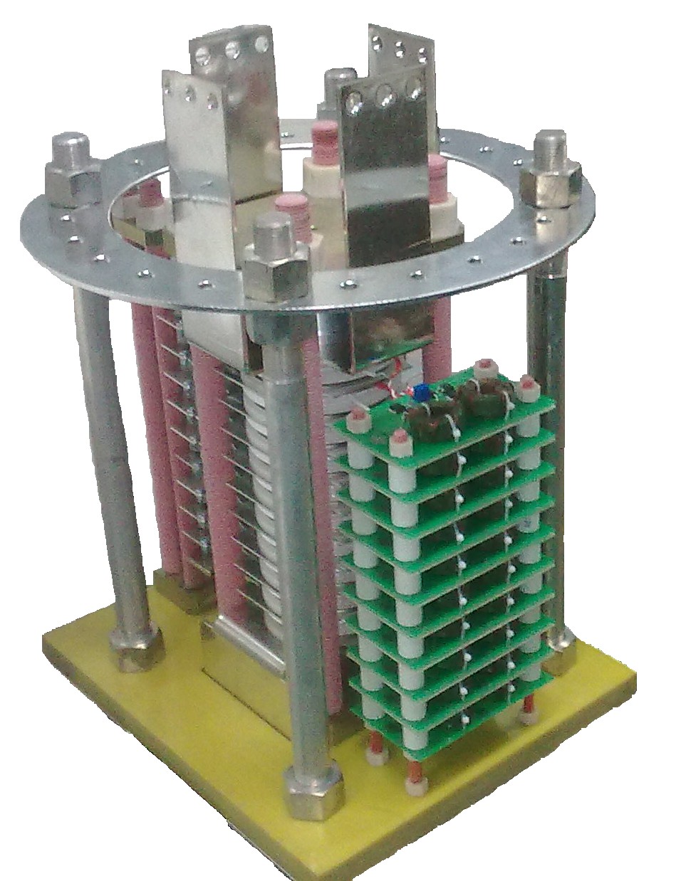
Fig. 7. Experimental thyristor switch for commutation of current pulse with 250 kA amplitude.
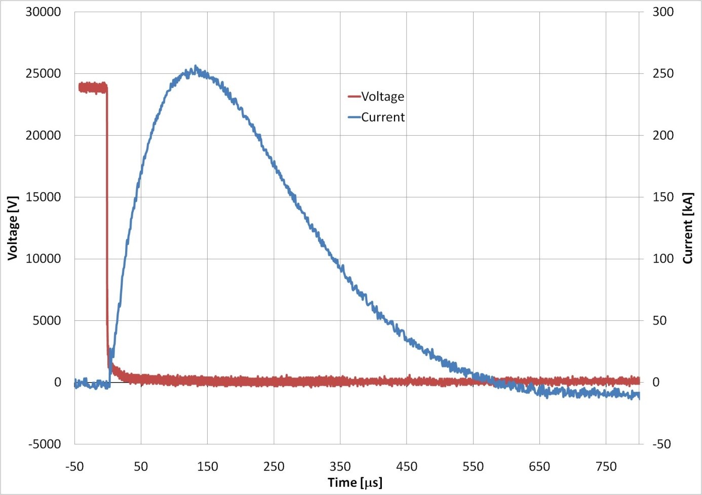
Fig. 9. . Oscilograph of current and voltage pulse commuted by the experimental switch produced on series connection 10 thyristors assembly.
CONCLUSION
There was developed the new generation of pulse silicon thyristors adapted to commute current impulses with extremely high amplitude, 100 – 1000 µs width. It was experimentally proved that it is possible for thyristor with 100 mm semiconductor element to commute current impulses with amplitude up to 250 kA and 500 µs width. New thyristors can be used to complete low cost solid state switches in pulse power supplies of high power electrophysical equipment.
REFERENCES
[1] M.E.Savage "Final Results From the High-Current, High-Action Closing Switch Test Program at Sandia National Laboratories", IEEE Transactions on Plasma Science, vol. 28, no. 5, pp. 1451-1455, Oct. 2000.
[2] H. Singh and C. R. Hummer “High action thyristors for pulse power applications”, in 12th IEEE Pulse Power Conference, June 1999.
[3] S. Ikeda and T. Araki, “ The di/dt capability of thyristors”, Proc. IEEE, no. 8, pp. 1301-1305, 1967.
[4] S.S. Asina, A.M. Surma, “A new design-technology technique for optimization of high power pulse thuristor characteristics”, in ELECTRIMACS Conference, Saint-Nazaire, Sept. 1996, pp. 485-490.
[5] W.H. Tobin, “Effect of gate configuration on thyristor plasma properties”, in IEE IAS Conference Record, IEE IAS Annual Meeting, 1978.
[6] Linder S., Klaka S. et al., "A New Range of Reverse Conducting Gate-Commutated Thyristors for High Voltage, Medium Power Applications", in EPE'97 Conference, pp. 1.117 - 1.124. 1997.
[7] A. V. Gorbatyuk, I. V. Grekhov, and A. V. Nalivkin, "Theory of quasidiode operation of reversely switched dinistors", Solid-State Electron., vol. 31 , pp. 1483-1491, 1988.
[8] S A. Belyaev, V.G. Bezuglov et al., “New Generation of High – Power Semiconductor Closing Switches for Pulsed Power Applications” in ICPIG Conference, Prague, July 2007.
[9] 1. H. Schwarzbauer, “Novel Large Area Joining Technique for Improved Power Device Performance”, IEEE Transactions on Industrial Applications, 27 (1), 1991, p. 93- 95.
[10] Amro R.; Lutz J. et al. “Power Cycling at High Temperature Swings of Modules with Low Temperature Joining Technique”, in ISPSD Conference, Naples, 2006.
[11] C. Göbl, P. Beckedahl, H. Braml, “Low temperature sinter technology Die attachment for automotive power electronic applications” in Automotive Power Electronics Conference, Paris, June 2006, pp. 2-5.
[12] D. Titushkin, A. Surma, “New ways to produce fast power thyristors”, Bodo’s Power Systems 08, 2015, p. 28- 29.


